I received two Ceres prototypes from JLCPCB earlier this month! Not wanting to smoke-test them in my Linux machine’s PCI Express slot, I wired them up using a PCIe-to-M.2 adapter, then an M.2-to-Thunderbolt adapter to my Mac. I connected the DC power supply, and… pop! The 0.85V switching regulator for main power to the FPGA let out its magic smoke. Turns out its enable pin had an internal pullup to +5V, and wasn’t designed to tolerate +12V.
RIP Ceres serial number 1.
On Ceres serial number 2, the relevant trace was too short to cut (it didn’t stick out far enough from under the regulator die), so I continued the bringup with a 5V power supply instead of the 12V one I’d intended to use. This time, there was no magic smoke, the FPGA showed up in Vivado, and I was able to program the QSPI Flash memory with a bitstream. Hooray!
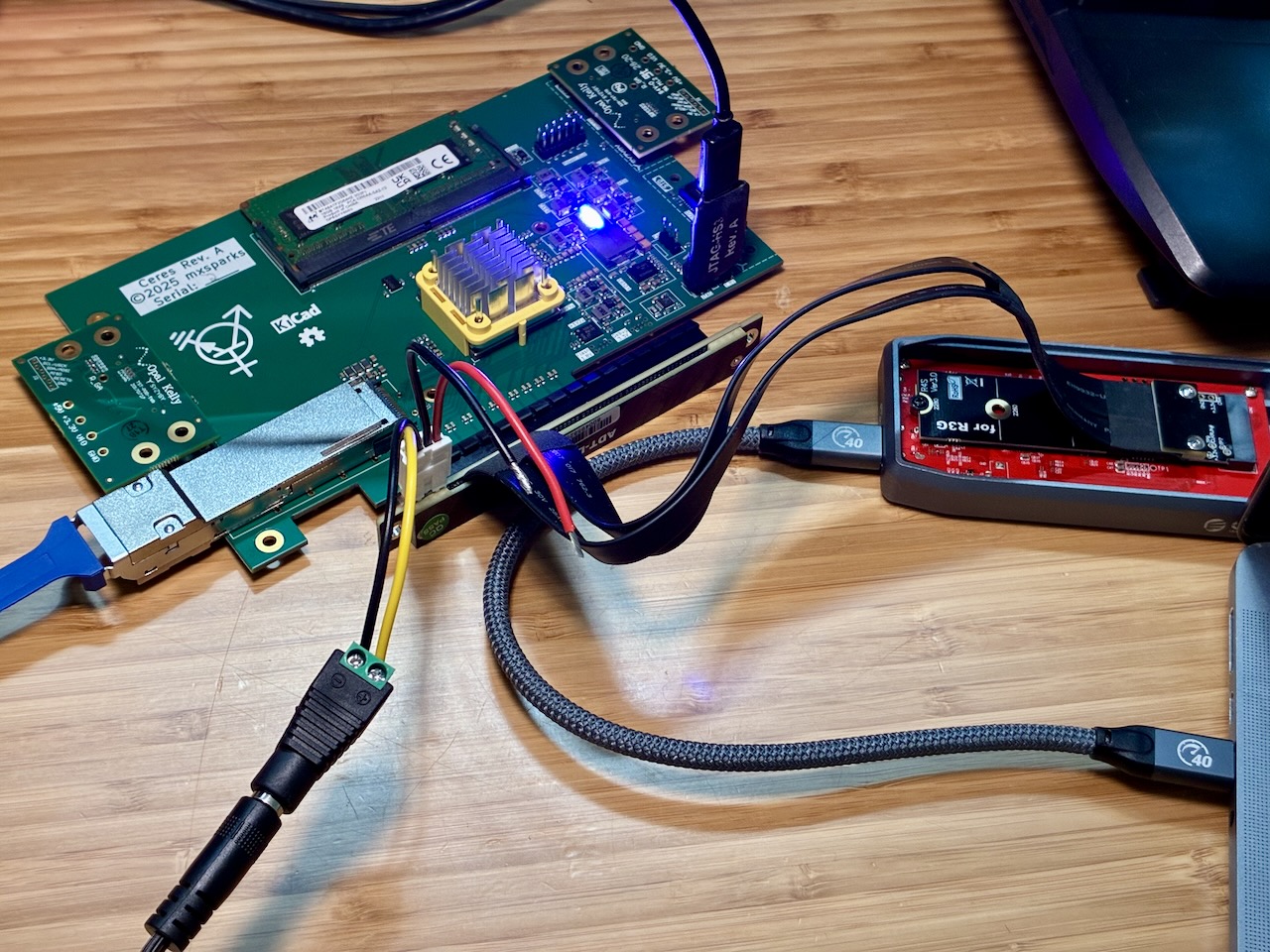
Except that the PCIe link never came up, and the DDR4 controller failed to train. Apparently that happens if your PCIe TX pairs are all swapped with the corresponding RX pairs, and if all your DDR4 clock and data strobes are polarity-inverted. I really should’ve commissioned one of my fellow EE friends to do a design review; it would’ve been cheaper than a board spin and taken less time.
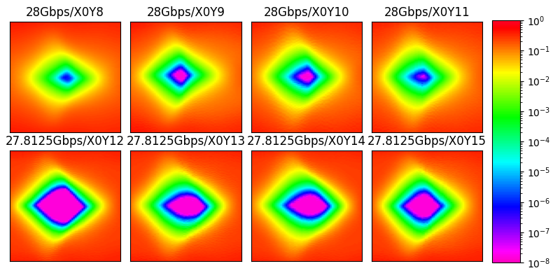
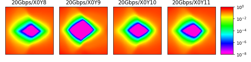
Fortunately, at least the SYZYGY and QSFP28 transceiver interfaces were connected properly, and I was able to test them using passive loopback modules. All four QSFP28 links were stable at 27.8125 Gbps with BER under 1e-12 and qualitatively good-looking statistical eye diagrams. The SYZYGY links were marginal at 28 Gbps with closed statistical eyes and BER around 1e-6, but rock-solid at 20 Gbps. (Samtec rates the SYZYGY TXR4 connectors for up to 19 Gbps.)
I also did some power-supply testing with a clip-on heatsink over the FPGA. For this test, I implemented an array of 65,536 ring oscillators to maximize power consumption, and a MicroBlaze RISC-V core running a proportional-control algorithm to keep supply voltage and junction temperature (as measured by the onboard ADC) and total system power (as measured by an INA226 current monitor) within limits. The plot below shows the number of active ring oscillators (“bbq”) over time, along with power consumption, Vccint supply voltage, and temperature.
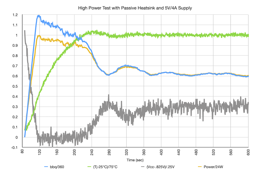
With the FPGA at ambient temperature, total power is limited by supply voltage droop to about 24 W, likely due to IR drop on the PCB between the 0.85V supply and the FPGA pins. The FPGA takes about two minutes to heat up to 100 C, at which point total power levels out around 15 W. Assuming 85% efficiency for the power delvery system, about 13 W is actually being dissipated by the FPGA heatsink. For revision B, I’ve moved the 0.85V regulator’s sense connection closer to the FPGA and ordered an active fan/heatsink; I’m hoping for closer to 40W thermal design power.
Changelog for revision B
I’ve made some other changes to fix minor problems, and I’m just waiting for parts availability before I place an order for revision B. Fingers crossed that this is what we go to production with!
- Leave U201 (0V85 regulator) enable pin floating
- Connect U201 sense pin closer to FPGA pads
- Change J201 (fan header) from through-hole to SMT
- Change J202 (power-out header) from pins to socket
- Change D301 (DONEn LED) from 3.3V to 1.8V
- Swap all J401 (DDR4 socket) DQSt/c and CKt/c pairs
- Swap all J501 (PCIe card edge) TX/RX lanes
- Remove ground fill between J501 pins
- Move J602 (QSFP cage) closer to board edge
- Use PTH for J701/J702/J703 (SYZYGY) pod mounting holes
- Clean up routing for J702 (SYZYGY TXR4) high-speed traces