It’s been a minute since the last update. Since then, I’ve received Rev.B prototypes of the Ceres FPGA dev board, and I’m pleased to report that both PCIe (Gen3 x8) and DDR4 are working! Unfortunately I still have some signal-integrity work to do for the DDR4 traces, as calibration is failing at speeds above 2000 MT/s and we really want to get 2400 MT/s out of this board. I’m not looking forward to trying to route the same number of tracks per millimeter with a bunch of additional via stitching; hopefully I don’t end up needing more layers on the PCB. Many thanks to @azonenberg for high-speed simulations and practical advice for opening up the eyes on the transceiver lanes as well.
PCIe testing is showing weirdly low bandwidth (less than 1GB/s) using AMD’s XDMA IP and the reference drivers on the host side. I suspect that might be due to a hardware bottleneck somewhere in my host PC; it’s an older Intel NUC, basically the cheapest thing I could find with a PCIe slot. I’ll have to benchmark it on my more powerful Mac using a PCIe to M.2 to Thunderbolt 3 adapter chain.
I also reran the ring-oscillator power test with a fancy fansink:
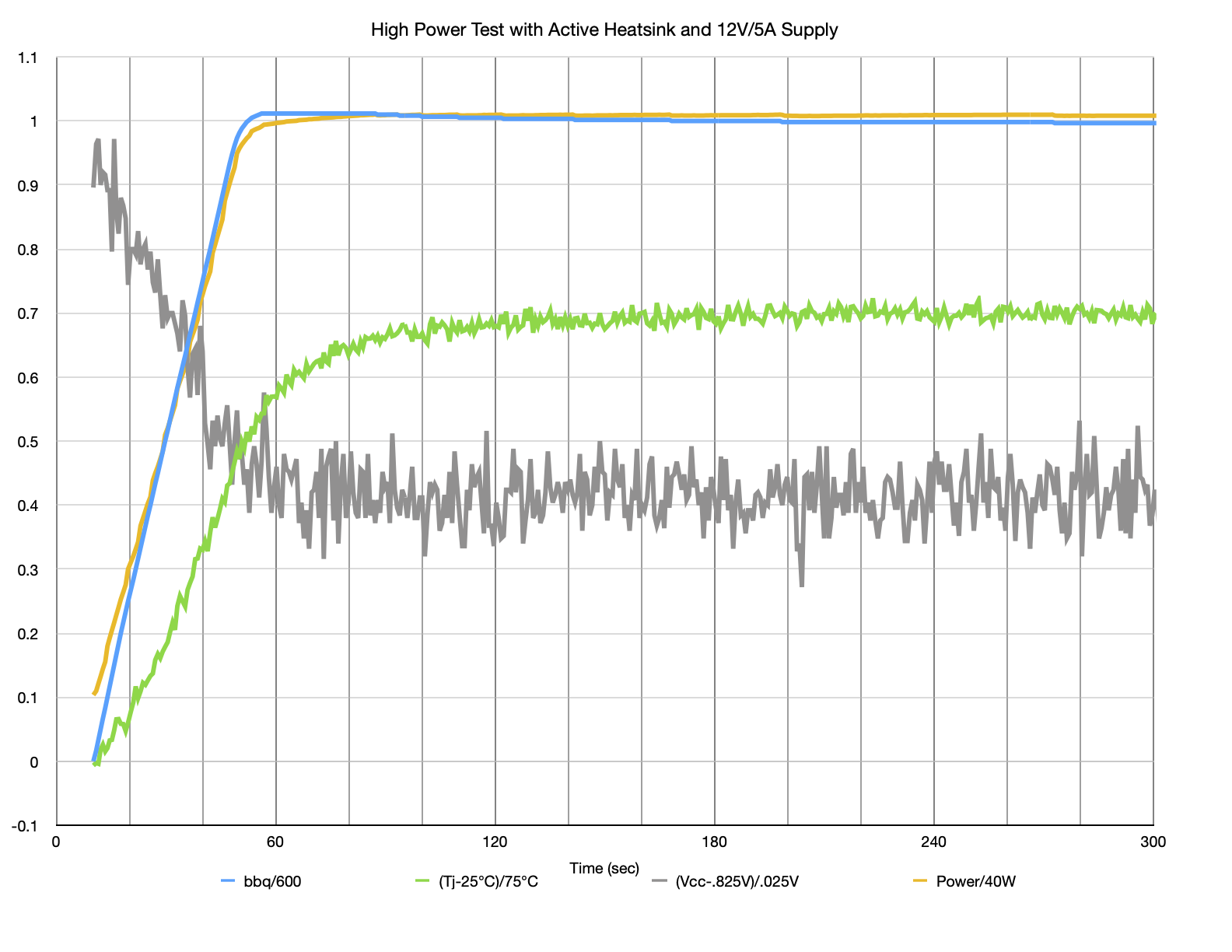 The 0.85V power supply on the board has its overcurrent protection set to
40A, and resets the board if that limit is exceeded. I set the board’s
target power consumption to 40W, just below where the overcurrent protection
triggered in practice. (This validates my assumption of about 85% power
supply efficiency.) The fansink I ordered was slightly oversized,
maintaining junction temperature around 77C at full power for a measured
θja (spoken “junction-to-ambient thermal resistance”) of just over 1.5 °C/W.
Supply voltage droop was still present, but much smaller after moving the
0.85V sense line closer to the FPGA pads instead of right next to the
regulator output.
The 0.85V power supply on the board has its overcurrent protection set to
40A, and resets the board if that limit is exceeded. I set the board’s
target power consumption to 40W, just below where the overcurrent protection
triggered in practice. (This validates my assumption of about 85% power
supply efficiency.) The fansink I ordered was slightly oversized,
maintaining junction temperature around 77C at full power for a measured
θja (spoken “junction-to-ambient thermal resistance”) of just over 1.5 °C/W.
Supply voltage droop was still present, but much smaller after moving the
0.85V sense line closer to the FPGA pads instead of right next to the
regulator output.